Depending on your design we produce semiconductor layer structures on 2 inch 3 inch 4 inch and 6 inch wafers. Techniques based on vacuum deposition vapor phase epitaxy and liquid and solid phase epitaxy are presented along with new techniques for the development of.
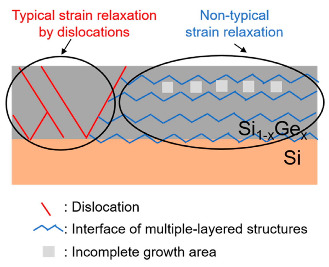 Applied Sciences Free Full Text Single Crystalline Si1
Cubic semiconductors strain relaxation by misfit dislocations strain and.
Epitaxy Of Semiconductor Layered Structures Volume 102 Book Pdf. Epitaxy of semiconductor layered structures. Liquid phase epitaxy lpe is a method to grow semiconductor crystal layers from the melt on solid substrates. The mrs symposium proceeding series is an internationally recognised reference suitable for researchers and practitioners.
Free shipping on qualifying offers. Volume 102 mrs proceedings r. The growth of copper silver and gold thin films on tungsten disulfide has been examined as a model of metal contacts on a layered semiconductor.
Hvpes featuresthe most well known being its fast growthrely on the use of chloride gaseous growth precursors as transport agents of the group iii elements. All three metals were found to grow epitaxially on the ws 2. We use two different reactors with 8 or 12 wafers per run to produce the wafers.
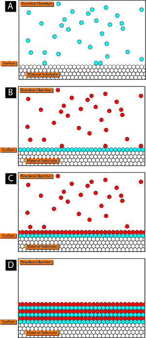
Alngan layered structures with layer periods between 15 and 40 nm have been grown on 0001 oriented sapphire and α6hsic substrates. In the early 1990s two approaches were developed to synthetize self assembled epitaxial semiconductor qds or artificial atomsnamely the stranskikrastanov sk and the droplet epitaxy. The growth was performed using a modified gas source molecularbeam epitaxy mbe technique.
Volume iiia focuses on major growth techniques which are used both in the scientific investigation of crystal growth processes and commercial development of advanced epitaxial structures. This happens at temperatures well below the melting point of the deposited semiconductor. However cu appears to form a discontinuous film while au and ag grow layer by layer.
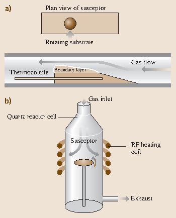
Hydride vapor phase epitaxy hvpe was part of the very first vapor phase epitaxy processes developed for the growth of iiiv semiconductor layers. The production of various components is based on the epitaxy of wafers. The semiconductor is dissolved in the melt of another material.
Standard effusion cells were used as sources of al and ga and a small mbe compatible electron cyclotron resonance ecr plasma source was used to activate. The book covers the structural and electronic properties of strained epitaxial layers the thermodynamics and kinetics of layer growth and the description of the major growth techniques metalorganic vapor phase epitaxy molecular beam epitaxy and liquid phase epitaxy. Excellent semiconductor material quality is an essential prerequisite for the fabrication of high power diode lasers and laser bars.
This review discusses issues in the epitaxial growth of semiconductor materials and layer sequences that form the basis for diode lasers.
 Heteroepitaxy Of Iiiv Zinc Blende Semiconductors On
 Epitaxial Crystal Growth Methods And Materials Springerlink
 Materials Special Issue Advances In Epitaxial Materials
 An Ultra Thin Buffer Layer For Ge Epitaxial Layers On Si
 Atomic Layer Deposition Wikipedia
 Robust Epitaxial Growth Of Two Dimensional Heterostructures
 Unleashing The Potential Of Molecular Beam Epitaxy Grown
Arxiv190206348v2 Physicsapp Ph 29 Mar 2019

 Epitaxial Crystal Growth Methods And Materials Springerlink
 Low Temperature Growth Of Fully Epitaxial Cofegefe3si
Epitaxial Growth Of Three Dimensionally Structured Iii V
 Epitaxy Of Small Organic Molecules Sciencedirect
 7 Epitaxial Layer Structure Of The Algangan Hemt 13


![[pdf] Free Download The City Seen As A Garden Of Ideas Book](https://lh3.googleusercontent.com/blogger_img_proxy/AEn0k_sq5jW5U1LEZoZFSZhp6MHigYgzIklVkefO6bGu7S4KYVZAw4pUfow3al-dHEPbE3r1oNZlHmZGCR002EAHAHJbbvxUXQWmw0NHjURDD1hHKOQ "[pdf] Free Download The City Seen As A Garden Of Ideas Book")


